Research details
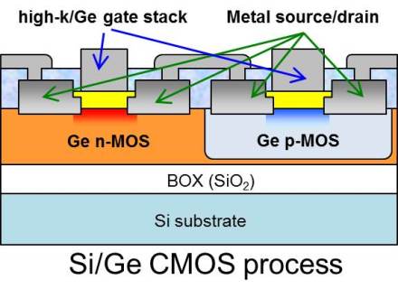
Si/Ge CMOS process technology
Complementary Metal-Oxide-Semiconductor (CMOS) transistor, which is an elementary device of Ultra Large Scale Integration (ULSI), was improved its performance by 3-dimensional downsizing technology called as “scaling.” However, because of restriction of Si’s material properties, nowadays it is difficult to improve its performance by simple scaling. Therefore, it is necessary to introduce booster technologies, such as 1) high permittivity (high-k) gate stack, 2) high mobility channel material, 3) decrease parasitic resistance of source/drain, and etc… We research such issues directly. Keywords) low temperature process for high quality gate stack, Ge channel, strain, SOI, GOI, metal source/drain
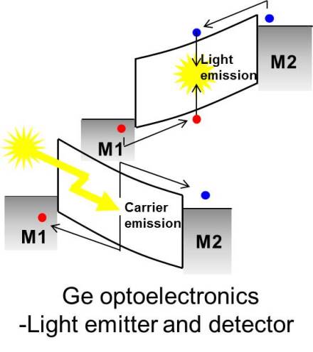
Ge optoelectronics
Ge, which has much higher electron and hole mobilities than those of Si, is attractive candidate of channel material for future CMOS. In addition, its direct energy bandgap is 0.80 eV which well corresponds light wavelength for optical communication (1.55 um). If we give Ge function of photoemission and detection, a way of Ge optical device will open. It means integration with Ge-CMOS, and wide applications such as optical interconnect will be expected. We have many original techniques concerning Ge process. Using these techniques, we study Ge optical device.
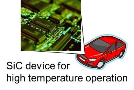
SiC process technology
Wide gap semiconductor such as 4H-SiC and GaN are received much attention as a basic material for power devices. On the other hand, another advantage of wide gap semiconductor is operation at high temperature. If CMOS operating at high temperature sets up around an engine of automotive, it is possible to actualize many benefits for example downsizing, simple wiring, and noise resistance. As a candidate material, we focus 3C-SiC (bandgap 2.2 eV). The reasons and advantages are 1) epitaxial growth on Si substrate, 2) high electron mobility, 3) appropriation of Si technology.

Ge novel electronic devices
"tunnel FET", "spin MOSFET", "flexible TFT"
Ge has unique feature such as "narrow bandgap", "low spin relaxation rate", and "low crystallization temperature". These feature has a potential applying to novel electronic devices. Based on our knowledge and experience through R&D of Ge CMOS process technology, we have started research about "tunnel FET", "spin MOSFET", and "flexible TFT".
・"Spin MOSFET" is collaborative research with Prof. Hamaya (Osaka Univ.) and Prof. Sawano (Tokyo City Univ.)
・"Flexible TFT" is collaborative research with Prof. Suemasu and Prof. Toko in Tsukuba Univ.
Underconstruction
2D materials device (collaborative research with Prof. Ago's lab. in GIC)
Move to Ago's lab. website
 Japanese
 English